
Bangalore is known as India’s Silicon Valley. With the fast growth of electronics, robotics, and automation industries, the demand for PCB board design in Bangalore has increased more than ever. From startups to big tech companies, everyone needs reliable PCBs that work smoothly. This is where choosing the right PCB partner matters.
Ettikengineering is one such trusted name that offers expert PCB design services in Bangalore. With years of experience and a skilled team, Ettik delivers high-quality PCBs for industries like aerospace, medical, automotive, and more.
Whether you are looking for a simple layout or a custom PCB board design in Bangalore, this blog will help you learn everything—from companies to avoid, to trends and processes you should know.
Best PCB Design Company in Bangalore
When it comes to choosing a PCB board design service in Bangalore, many companies claim to be the best. But only one truly delivers consistent quality, precision, and timely results is Ettikengineering. Ettik offers end to end custom PCB solutions with expert engineers, fast turnaround and strong support. Serving sectors like robotics, defense, and industrial automation, Ettik leads the way in design and delivery.
Want to know why we are the best? Click the link below to find out.
Choose the Right PCB Board Design Service in Bangalore
Before finalizing your PCB design partner, here are some key things you should consider:
- Experience: How long have they been designing PCBs?
- Custom Capabilities: Can they handle custom PCB board design in Bangalore?
- Prototyping Support: Do they offer early testing before mass production?
- Turnaround Time: How fast can they deliver your PCB?
- Testing and Quality Check: Do they test all boards before delivery?
Quick Checklist:
- Years of experience
- PCB design + manufacturing under one roof
- Quick prototyping options
- Certifications (ISO, IPC, etc.)
- Fast delivery time and full support
When choosing the right PCB design service in Bangalore, Ettik ticks all the boxes.
PCB Manufacturing Process Explained
If you’re new to the PCB world, don’t worry. Here’s a simple step-by-step breakdown of how PCBs are designed and built:
- Requirement Analysis – Understand the electrical needs of your project.
- Schematic Design – Draw the circuit diagram with all components.
- PCB Layout – Convert the circuit into a board layout (tracks, pads, holes).
- Simulation & Review – Test the design virtually for errors.
- Creation – Build the first sample board.
- Testing – Check the prototype for performance, signal flow, and errors.
- Final Production – Once approved, begin mass production.
Understanding the PCB design process in Bangalore is helpful when working with companies like Ettik. They guide you at each step, ensuring the board meets your project’s needs.
Latest Trends in PCB Design Technology (2025)
Technology is always changing, and PCB design is no different. Here are the top PCB design trends in 2025 you should know:
- Miniaturization: PCBs are getting smaller but more powerful.
- High-Density Interconnect (HDI): Supports more components in less space.
- AI in PCB Design: Tools now use artificial intelligence to avoid layout errors.
- IoT-Ready Boards: Boards are now designed for smart, connected devices.
- 3D PCB Layouts: Helps in better thermal control and compact design.
Ettik Engineering has already adopted these technologies in its latest projects. If you’re planning a custom PCB board design in Bangalore, you need a partner who understands these latest trends.
Common Mistakes in PCB Design and How to Avoid Them
Even the smallest mistake in PCB design can cause major issues. Here are 5 common errors and how Ettik avoids them:
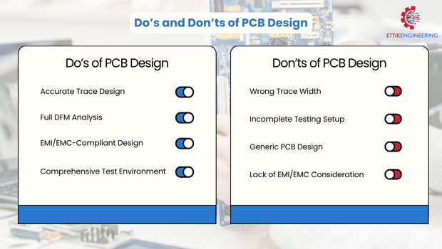
- Incorrect Component Placement
Ettik uses software tools and manual checks to ensure proper layout. - Wrong Trace Widths
Correct widths are chosen based on current flow and voltage. - Missing Ground Planes
Proper grounding reduces noise and improves signal quality. - Poor Thermal Management
Heat-sensitive components are placed smartly. - No DFM Check (Design for Manufacturing)
Ettik runs full DFM analysis before production begins.
Avoiding these PCB design mistakes and solutions ensures that your project runs smoothly from day one.
Why Ettik Engineering is a Trusted PCB Design Partner in Bangalore
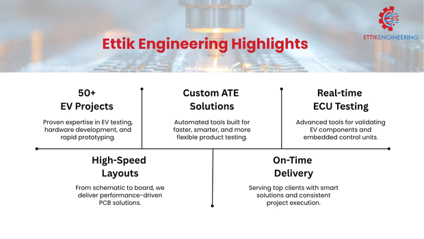
So, why do top companies trust Ettik?
- Industries Served: Automotive, Aerospace, Medical, Consumer Electronics, Robotics.
- Project Success: 50+ successful projects delivered with 98% on-time completion rate.
- Client Testimonials: Clients praise Ettik’s design accuracy and responsive support.
- In-House Lab: Offers real-time testing and faster revisions.
- Custom Solutions: Each design is tailor-made for the client’s needs.
If you’re looking for a trusted PCB design company in Bangalore, Ettik has proven experience and happy clients to back its reputation.
From understanding the PCB board design process in Bangalore to selecting the right partner, we’ve covered all you need to know. Whether you’re a startup or a large company, choosing the right PCB design team can save time, cost, and errors.
Ready to build your next PCB project with a trusted partner?
Get a free PCB design consultation from Ettik Engineering today.