
If you’re building any kind of electronic product, the PCB board design is the heart of your device. Whether it’s a small gadget or a complex machine, the Printed Circuit Board (PCB) connects and powers every component inside. For businesses looking for PCB board design in Bangalore, this guide will help you understand the complete process from idea to final product.
At EttikEngineering, we offer custom PCB board design in Bangalore and full manufacturing support to bring your product to life, faster and smarter.
What Is a PCB and Why It’s Important?
A PCB or Printed Circuit Board, is a flat board that holds all the electronic parts together and allows them to connect. You’ll find PCBs inside:
- Phones
- TVs
- Cars
- Computers
- Industrial machines
It helps power the device, manage signals, and make sure everything runs smoothly.
Choosing a trusted PCB board design service in Bangalore is the first step in making sure your product works well and lasts long.
Step by Step PCB Design Process
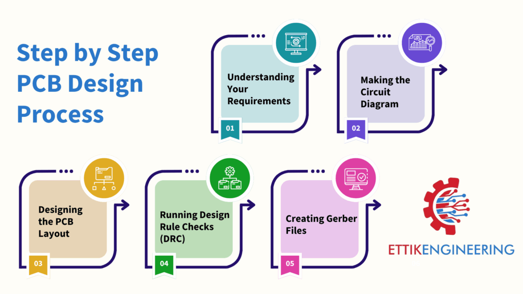
1. Understanding Your Requirements
Before we start designing, we sit with you and understand:
- What does your product need to do?
- What are the size limits?
- How many components are required?
This step helps in creating a good plan for the full design.
2. Making the Circuit Diagram (Schematic)
Our engineers draw a basic electronic map of your product. It shows how all parts connect. We use tools like Altium or KiCad to create the schematic.
This is the first step in PCB design services in Bangalore, and it builds the base for the whole design.
3. Designing the PCB Layout
Now we move the circuit from paper to the board. We place all parts on a virtual board and draw the paths (called traces) that connect them.
Good layout design makes sure:
- Signals move without delay
- Parts do not overheat
- The board fits in your product
EttikEngineering has years of practice in custom PCB board design Bangalore clients trust for both simple and complex devices.
4. Running Design Rule Checks (DRC)
We use software to check:
- Are the traces too close?
- Are all parts connected?
- Will this design work in real life?
Only after this step, we move to manufacturing.
5. Creating Gerber Files
We generate Gerber files — these are like a digital blueprint sent to the factory. These files tell the machine:
- Where to place holes
- Where to cut the board
- Where to print copper lines
At EttikEngineering, we double check every Gerber file to avoid errors in production.
The PCB Manufacturing Process
Once the design is ready, the board goes to production. Here’s what happens step by step:
1. Selecting Material
We choose the right material (usually FR4) based on your needs whether you need speed, strength, or flexibility.
2. Printing the Circuit Pattern
We use machines to print the copper layout on the board. The unwanted copper is removed through etching.
3. Drilling Holes
Tiny holes are drilled where components will be placed. High-speed drills are used for this.
4. Adding Layers and Plating
If your board has more than one layer (multilayer PCB), we line up the layers and add copper plating to connect them.
5. Solder Mask and Silkscreen
The solder mask covers the board to protect it. The silkscreen prints labels and part numbers.
6. Surface Finishing
The board gets a final finish like HASL or ENIG, which protects copper and improves soldering.
7. Quality Testing
We test for:
- Short circuits
- Open connections
- Board shape and size
All our PCB board design services in Bangalore come with strict quality checks at each step.
How Much Does PCB Design Cost in Bangalore?

Here’s the truth:
| Service | Price Range | Best For |
| Simple 2-layer design | ₹15,000-30,000 | Hobby projects |
| 4-layer complex board | ₹50,000-1,20,000 | Professional products |
| Full turnkey service | ₹300/board+ | Large orders |
Warning: If someone quotes ₹5,000 for a 4-layer design, they’re probably cutting corners.
Why Choose Our PCB Design Services in Bangalore?
There are many companies that say they offer PCB design services in Bangalore. So why choose us?
Here’s what makes EttikEngineering the right choice:
- 10+ years of PCB experience
- Custom designs for startups and large companies
- Fast turnaround time
- 100% in-house design and testing
- Transparent pricing, no hidden charges
We have worked with over 100 electronics brands, helping them build reliable products with quality custom PCB board design in Bangalore.
Mistakes to Avoid in PCB Design
- Putting too many parts too close
– Causes overheating or short circuits. - Bad routing of signals
– Leads to signal delay or noise. - Not testing before production
– Always run checks using simulation tools. - Ignoring manufacturing limits
– We design for both function and manufacturability.
With EttikEngineering, our team avoids these common issues by following global PCB standards and smart design methods.
What Does PCB Design and Manufacturing Cost?
The price depends on:
- Board size
- Number of layers
- Part types
- Quantity
For simple boards, costs start around ₹3,000. More complex boards can go higher. We also offer cost-effective options for startups or first-time makers.
Our goal is to give you value, not just a product. That’s why so many trust our PCB board design service in Bangalore.
Startup to Market in 21 Days
One startup came to us with just an idea. They needed a working PCB in 3 weeks.
- Day 1: Schematic and layout
- Day 7: Gerber files ready
- Day 15: Board manufactured and assembled
- Day 21: Testing completed
Result? A working prototype in 21 days. They launched their product in just 2 months — 40% faster than their competitors.
This is the power of working with a team that knows PCB design services in Bangalore inside out.
Frequently Asked Questions
Q1: Can I get a sample before full production?
Yes. We always suggest making a prototype first.
Q2: Do you support multilayer boards?
Yes, up to 12 layers and custom shapes.
Q3: What tools do you use for design?
We use industry tools like Altium, KiCad, Eagle, and more.
Q4: How do I get started with EttikEngineering?
Just send your idea or schematic. We’ll take it from there.
Get Your PCB Board
At EttikEngineering, best PCB Design Company in Bangalore we don’t just design we guide, build and support. Whether you’re launching a new product or improving an old one, our PCB board design services in Bangalore are here to help.
Contact us today
Get a free quote