Nowadays, almost every electronic device like a smartwatch or even an electric car works because of one main part: the printed circuit board (PCB). As technology becomes faster and smaller, the need for multilayer PCBs has grown rapidly.
At Ettikengineering, we specialize in pcb board design in Bangalore, creating smart, compact, and reliable boards that power modern electronics. This article will help you understand what multilayer PCBs are, their benefits, and the challenges engineers face while designing them.
In this article, you’ll learn:
- Why multilayer PCBs are vital for modern electronics
- The real benefits and design challenges
- How Ettik’s PCB design services in Bangalore solve common PCB testing issues
Multilayer PCB Design in Bangalore
A multilayer PCB is a board made up of several layers of copper and insulation stacked together. These extra layers allow more components and signal paths to fit into a smaller space.
Unlike single-layer PCBs, multilayer boards support advanced features and faster performance. They are used in devices like medical instruments, industrial controllers, automotive systems, and communication equipment.
| Multilayer PCB Quick FactsType: Printed Circuit Board with 3+ conductive layers Used in: Automotive, Aerospace, Medical and Consumer Electronics Key Benefit: Compact design, higher signal integrity Offered by: Ettikengineering — leading PCB board design in Bangalore Category: Electronics Manufacturing & Testing |
Our team at Ettikengineering provides PCB design services in Bangalore that follow global standards, ensuring every design performs smoothly and reliably in real-world applications.
Key Benefits of Multilayer PCB Design
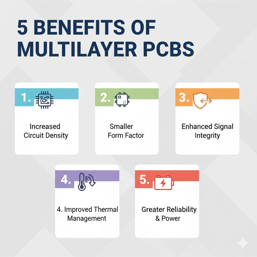
1. Compact and Powerful
Multilayer PCBs allow engineers to pack more circuits into less space. This makes them ideal for smartphones, EV controllers, and aerospace devices.
With custom PCB board design Bangalore, we help clients reduce product size while increasing performance and speed.
2. Improved Electrical Performance
Multiple layers mean shorter signal paths, which reduce noise and interference. This improves signal integrity and ensures stable performance.
Ettikengineering’s PCB Board Design Service in Bangalore uses advanced design tools to maintain perfect alignment between layers, resulting in better connectivity and minimal data loss.
3. Greater Reliability
Because of their strong structure and laminated layers, multilayer PCBs are more durable and long-lasting. They can handle high temperatures and demanding industrial environments.
| Type | Layers | Cost | Application |
| Single Layer PCB | 1 | Low | Simple electronics |
| Double Layer PCB | 2 | Medium | LED panels, sensors |
| Multilayer PCB | 4+ | High | Industrial, automotive, IoT devices |
Challenges in Multilayer PCB Design
While multilayer PCBs offer many advantages, they also come with certain challenges:
- Complex Layer Management: Proper layer arrangement is important for power and signal flow.
- Thermal Issues: Multiple layers create more heat, which must be managed efficiently.
- Testing Difficulty: As the number of layers increases, it becomes harder to detect faults manually.
That’s why Ettikengineering uses automated testing systems to ensure zero defects in every board. Whether you need pcb board design in Bangalore for industrial automation or high-speed communication, we make sure your boards are tested and ready for production.
| 💡 Did You Know? The first multilayer PCB was built in the 1960s for military radar systems. |
Our Design Process
At Ettikengineering, we follow a detailed process for every custom PCB board design Bangalore project:
- Requirement Study: Understanding your product and circuit needs.
- Schematic Design: Translating your idea into a clear electrical design.
- Layer Stack-Up Planning: Deciding how many layers are needed for best performance.
- Routing and Simulation: Ensuring signal paths are clean and noise-free.
- Fabrication & Testing: Delivering tested, production-ready PCB boards.
Our experienced engineers handle each step carefully to ensure accuracy, speed, and performance.
| Industry | Typical PCB Layers | Special Requirement |
| Automotive | 6–10 | Heat resistance |
| Medical | 4–8 | High reliability |
| Aerospace | 8–12 | Signal accuracy |
| Consumer | 4–6 | Compact size |
Why Choose Ettikengineering
Ettikengineering is a trusted name for PCB Board Design Service in Bangalore. Here’s why clients choose us:
- End-to-end PCB design services in Bangalore, from concept to testing.
- Expertise in multilayer, high-density, and custom PCB board design Bangalore.
- Advanced testing systems that ensure quality and reliability.
- Fast delivery and flexible design support for startups and enterprises alike.We combine design knowledge, automation, and engineering experience to help you bring your product ideas to life.
Multilayer PCB design plays a key role in today’s electronics industry. While it offers great performance and space savings, it also needs skilled engineers to manage design complexity and testing accuracy.
| PCB Design Growth in Bangalore Bangalore is India’s electronics hub. Companies like Ettikengineering are driving innovation in PCB board design in Bangalore, providing world-class testing and automation solutions for OEMs and startups. |
At Ettikengineering, we provide expert pcb board design in Bangalore that balances innovation, cost, and performance. Whether you’re developing a new electronic product or improving an existing one, our PCB design services in Bangalore can help you achieve the perfect balance of reliability and efficiency.
Get in touch with Ettikengineering today to discuss your next custom PCB board design Bangalore project and experience the difference that precision engineering can make.
People Also Ask
1. Why are multilayer PCBs better than single-layer boards?
They provide more circuit density, higher performance, and better EMI control.
2. What industries use multilayer PCBs the most?
Automotive, aerospace, consumer electronics, and industrial automation.
3. How does Ettik Engineering test multilayer PCBs?
Through automated test systems ensuring zero defects and full performance validation.
Related Blogs
Ettikengineering
Website | Directions | Instagram | Medium | Whatsapp
Phone: +91 7418619304
Address:D.No 172/175 ,1St Floor,Paramathi Road,S.P Pudur, Namakkal -637001 Tamil Nadu, india.